
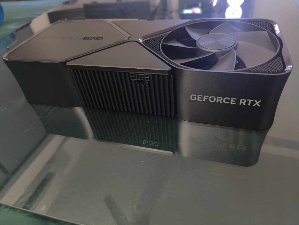
Rumors are circulating that the upcoming NVIDIA GeForce RTX 5090 will showcase a TBP (Total Board Power) of up to 600W. This information originates from the reputable source @kopite7kimi, who asserts that the Blackwell gaming flagship is projected to have a maximum power rating of 600 watts. This is a substantial increase of 150W compared to the RTX 4090, the current fastest gaming GPU. Conversely, it’s reported that the RTX 5080 will launch with a TBP of 400 watts, a step up from the 320W seen in the RTX 4080 and the 4080 Super.
The GeForce RTX 5090 is set to utilize the GB202 GPU architecture, comprised of 12 GPCs (Graphics Processing Clusters), each housing 8 TPCs (Texture Processing Clusters). A TPC includes two SMs (Streaming Multiprocessors) or 256 FP32 cores, equating to a total shader count of 24,576 for the GB202.
The GB202 will be paired with 16 GDDR7 memory modules via a 512-bit bus, delivering between 28GB and 32GB of graphics memory, contingent on the bus width. Depending on the desired performance metrics, NVIDIA might opt for a 384-bit, 448-bit, or the full 512-bit memory bus for the RTX 5090. With 28 Gbps of GDDR7 graphics memory across a 512-bit bus, an external memory bandwidth of 1568GB/s is achieved.
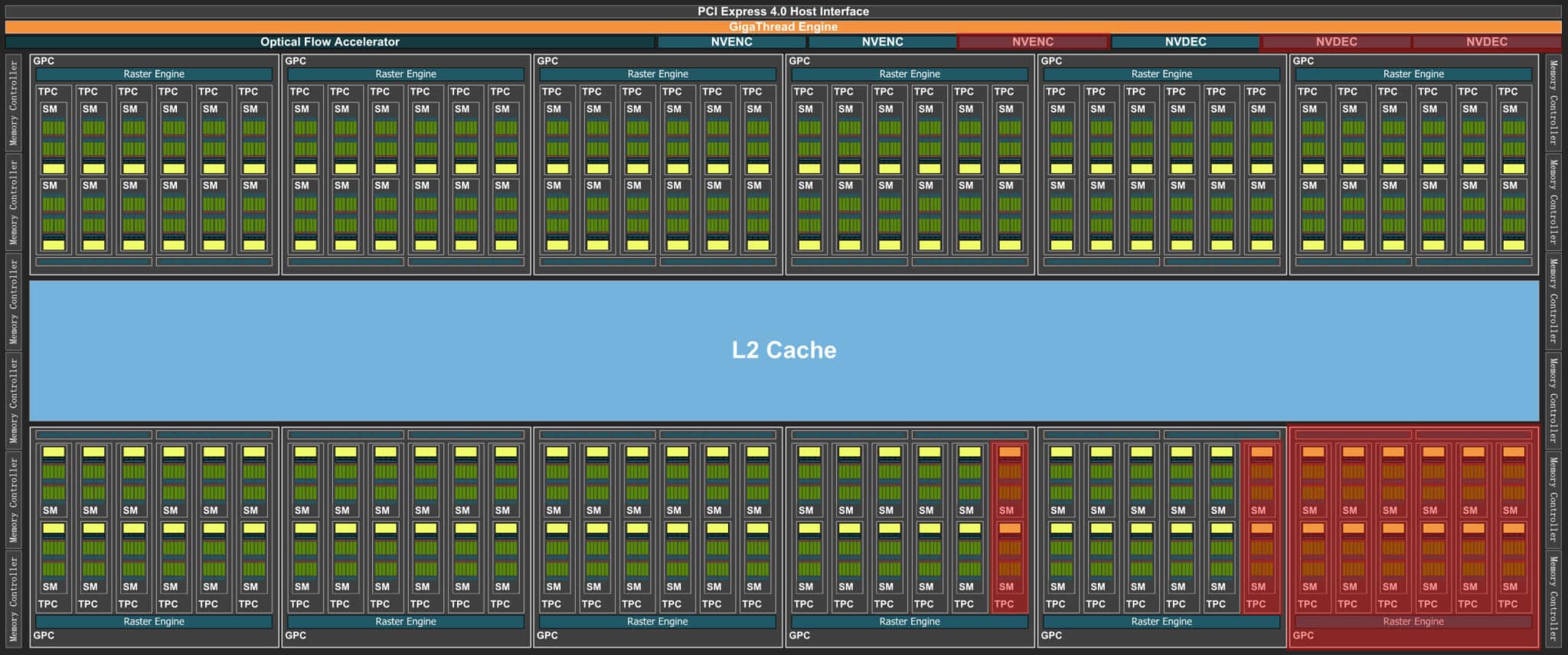
Expected on the shader side are 17000-20000 FP32 cores (equivalent to 133 to 156 SMs), suggesting the presence of 2 fully or 4 partially disabled GPCs. The L2 cache is anticipated to scale in line with the shader and memory bus, potentially reaching around ~128MB for the highest-end SKU.
Regarding the GeForce RTX 5080, reports indicate that it will sport a similar shader setup to the 4080, featuring 7 GPCs, each incorporating 6 TPCs or 12 SMs. This results in an overall core count of 10752, an increase from 10240 found in the AD103 and the RTX 4080 Super. The bus width, resting at 256 bits, remains unchanged, but the speedier GDDR7 memory is expected to enhance the external bandwidth to as much as 896GB/s (up from 736GB/s seen with the RTX 4080 Super).
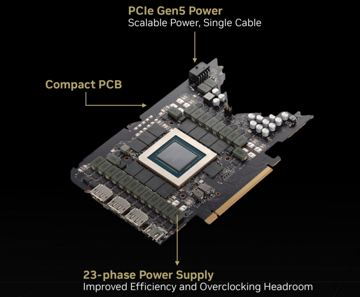
A recent report by mydrivers details how NVIDIA had to revamp the upper metal layers and connections of its GPUs dedicated to gaming and AI. The motive behind this overhaul was an inconsistency in the coefficient of thermal expansion (CTE) among the GPU die, LSI bridging, RDL interposer, and the primary substrate, which could potentially result in chip distortion and system malfunction. The updated TBPs accompanying the redesign are likely aimed at optimizing the performance targets following a postponed release schedule.